


EN 60191-6-18:2010
(Main)Mechanical standardization of semiconductor devices - Part 6-18: General rules for the preparation of outline drawings of surface mounted semiconductor device packages - Design guide for ball grid array (BGA)
General Information
- Abstract
IEC 60191-6-18:2010 provides standard outline drawings, dimensions, and recommended variations for all square ball grid array packages (BGA), whose terminal pitch is 1 mm or larger.
- Status
- Published
- Publication Date
- 25-Feb-2010
- Withdrawal Date
- 31-Jan-2013
- Technical Committee
- CLC/TC 47X - Semiconductor devices and trusted chips
- Drafting Committee
- IEC/SC 47D - IEC_SC_47D
- Parallel Committee
- IEC/SC 47D - IEC_SC_47D
- Current Stage
- 6060 - Document made available - Publishing
- Start Date
- 26-Feb-2010
- Completion Date
- 26-Feb-2010



Overview
EN 60191-6-18:2010 is a European standard developed by CENELEC (CLC), aligned with IEC 60191-6-18:2010, focusing on the mechanical standardization of semiconductor devices. Specifically, this standard provides general rules and a comprehensive design guide for the preparation of outline drawings of surface mounted semiconductor device packages, with particular emphasis on ball grid array (BGA) packages with a terminal pitch of 1 mm or larger. The document aims to establish standardized practices for the dimensions, outline drawings, and recommended variations for square BGA packages, ensuring consistency and interchangeability across the electronics industry.
Key Topics
Some essential topics addressed in EN 60191-6-18:2010 include:
- Standard Outline Drawings: Guidelines for the creation of mechanical outline drawings for square BGA packages, establishing a uniform format for documentation and communication.
- Package Dimensions and Variations: Specification of key dimensions (length, width, pitch, height, terminal position) and their permissible variations for BGA devices, contributing to effective standardization.
- Terminal Numbering and Matrix Arrangement: Clear rules for terminal position numbering, using alphanumeric identification for rows and columns, supporting ease of reference in manufacturing and inspection.
- Recommended BGA Variations: Introduction of preferred BGA outline and ball count configurations to minimize proliferation of custom packages and support streamlined production.
- Symbolism and Drawing Guidance: Standardized symbols and annotation methods explained to ensure drawings are universally understood and unambiguous.
- Tolerance and Coplanarity Requirements: Critical tolerances for body dimensions, terminal positions, and coplanarity, helping ensure high-quality soldering and reliable assembly.
- Terminology Clarification: Definitions of key terms related to BGA types, such as P-BGA (plastic), T-BGA (tape), and C-BGA (ceramic), fostering common understanding.
Applications
EN 60191-6-18:2010 is widely applicable across the semiconductor and electronics sectors, especially in:
- Semiconductor Device Manufacturing: Supporting design, development, and quality assurance of BGA packages used in integrated circuits, memory devices, and processors.
- PCB Assembly and Design: Providing necessary references for printed circuit board (PCB) designers and assembly engineers to ensure compatibility with standardized BGA footprints.
- Component Suppliers and Distributors: Enabling consistent packaging and datasheet preparation for a broad market base.
- Testing and Inspection: Facilitating automated and manual measurement processes by defining critical dimensioning and tolerances, ensuring components meet standardized criteria.
- Global Supply Chain Operations: Promoting seamless interchangeability of devices among suppliers, contract manufacturers, and OEMs by removing ambiguities in mechanical specifications.
Related Standards
For comprehensive implementation and reference, the following related standards should also be considered:
- IEC 60191-6: General rules for the preparation of outline drawings of SMD semiconductor device packages.
- IEC 60191-6-2: Design guide for ball and column terminal packages with pitches of 1.50 mm, 1.27 mm, and 1.00 mm.
- IEC 60191-6-4: Measuring methods for package dimensions of ball grid arrays (BGA).
- IEC 60191-6-5: Design guide for fine-pitch ball grid array (FBGA) packages.
Summary of Practical Value
Adopting EN 60191-6-18:2010 assures clear communication in the design and production of BGA packages for surface-mount technology (SMT), reduces the risk of incompatibility and rework, and simplifies international trade in semiconductor devices. This standard helps stakeholders across design, manufacturing, and supply chain management optimize interoperability, efficiency, and reliability for semiconductor products utilizing BGA packages.
Relations
- Effective Date
- 03-Feb-2026
Frequently Asked Questions
EN 60191-6-18:2010 is a standard published by CLC. Its full title is "Mechanical standardization of semiconductor devices - Part 6-18: General rules for the preparation of outline drawings of surface mounted semiconductor device packages - Design guide for ball grid array (BGA)". This standard covers: IEC 60191-6-18:2010 provides standard outline drawings, dimensions, and recommended variations for all square ball grid array packages (BGA), whose terminal pitch is 1 mm or larger.
IEC 60191-6-18:2010 provides standard outline drawings, dimensions, and recommended variations for all square ball grid array packages (BGA), whose terminal pitch is 1 mm or larger.
EN 60191-6-18:2010 is classified under the following ICS (International Classification for Standards) categories: 31.080.01 - Semiconductor devices in general. The ICS classification helps identify the subject area and facilitates finding related standards.
EN 60191-6-18:2010 has the following relationships with other standards: It is inter standard links to EN 60191-6:2009. Understanding these relationships helps ensure you are using the most current and applicable version of the standard.
EN 60191-6-18:2010 is available in PDF format for immediate download after purchase. The document can be added to your cart and obtained through the secure checkout process. Digital delivery ensures instant access to the complete standard document.
Standards Content (Sample)
2003-01.Slovenski inštitut za standardizacijo. Razmnoževanje celote ali delov tega standarda ni dovoljeno.Mechanische Normung von Halbleiterbauelementen - Teil 6-18: Allgemeine Regeln für die Erstellung von Gehäusezeichnungen von SMD-Halbleitergehäusen - Konstruktionsleitfaden für Ball-Grid-Array (BGA) (IEC 60191-6-18:2010)Normalisation mécanique des dispositifs à semiconducteurs - Partie 6-18: Règles générales pour la préparation des dessins d'encombrement des dispositifs à semiconducteurs pour montage en surface - Guide de conception pour les boîtiers matriciels à billes (BGA) (CEI 60191-6-18:2010)Mechanical standardization of semiconductor devices - Part 6-18: General rules for the preparation of outline drawings of surface mounted semiconductor device packagers - Design guide for ball grid array (BGA) (IEC 60191-6-18:2010)31.240Mehanske konstrukcije za elektronsko opremoMechanical structures for electronic equipment31.080.01Polprevodniški elementi (naprave) na splošnoSemiconductor devices in general01.100.25Electrical and electronics engineering drawingsICS:Ta slovenski standard je istoveten z:EN 60191-6-18:2010SIST EN 60191-6-18:2010en,fr01-april-2010SIST EN 60191-6-18:2010SLOVENSKI
STANDARD
EUROPEAN STANDARD EN 60191-6-18 NORME EUROPÉENNE
EUROPÄISCHE NORM February 2010
CENELEC European Committee for Electrotechnical Standardization Comité Européen de Normalisation Electrotechnique Europäisches Komitee für Elektrotechnische Normung
Central Secretariat: Avenue Marnix 17, B - 1000 Brussels
© 2010 CENELEC -
All rights of exploitation in any form and by any means reserved worldwide for CENELEC members.
Ref. No. EN 60191-6-18:2010 E
ICS 31.080.01
English version
Mechanical standardization of semiconductor devices -
Part 6-18: General rules for the preparation of outline drawings
of surface mounted semiconductor device packages -
Design guide for ball grid array (BGA) (IEC 60191-6-18:2010)
Normalisation mécanique
des dispositifs à semiconducteurs -
Partie 6-18: Règles générales
pour la préparation des dessins d'encombrement des dispositifs
à semiconducteurs
pour montage en surface -
Guide de conception pour les boîtiers matriciels à billes (BGA) (CEI 60191-6-18:2010)
Mechanische Normung
von Halbleiterbauelementen -
Teil 6-18: Allgemeine Regeln
für die Erstellung
von Gehäusezeichnungen
von SMD-Halbleitergehäusen -
Konstruktionsleitfaden
für Ball-Grid-Array (BGA) (IEC 60191-6-18:2010)
This European Standard was approved by CENELEC on 2010-02-01. CENELEC members are bound to comply with the CEN/CENELEC Internal Regulations which stipulate the conditions for giving this European Standard the status of a national standard without any alteration.
Up-to-date lists and bibliographical references concerning such national standards may be obtained on application to the Central Secretariat or to any CENELEC member.
This European Standard exists in three official versions (English, French, German). A version in any other language made by translation under the responsibility of a CENELEC member into its own language and notified to the Central Secretariat has the same status as the official versions.
CENELEC members are the national electrotechnical committees of Austria, Belgium, Bulgaria, Croatia, Cyprus, the Czech Republic, Denmark, Estonia, Finland, France, Germany, Greece, Hungary, Iceland, Ireland, Italy, Latvia, Lithuania, Luxembourg, Malta, the Netherlands, Norway, Poland, Portugal, Romania, Slovakia, Slovenia, Spain, Sweden, Switzerland and the United Kingdom.
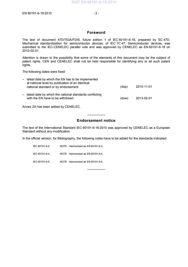
Foreword The text of document 47D/753A/FDIS, future edition 1 of IEC 60191-6-18, prepared by SC 47D, Mechanical standardization for semiconductor devices, of IEC TC 47, Semiconductor devices, was submitted to the IEC-CENELEC parallel vote and was approved by CENELEC as EN 60191-6-18 on 2010-02-01. Attention is drawn to the possibility that some of the elements of this document may be the subject of patent rights. CEN and CENELEC shall not be held responsible for identifying any or all such patent rights. The following dates were fixed: – latest date by which the EN has to be implemented
at national level by publication of an identical
national standard or by endorsement
(dop)
2010-11-01 – latest date by which the national standards conflicting
with the EN have to be withdrawn
(dow)
2013-02-01 Annex ZA has been added by CENELEC. __________ Endorsement notice The text of the International Standard IEC 60191-9-18:2010 was approved by CENELEC as a European Standard without any modification. In the official version, for Bibliography, the following notes have to be added for the standards indicated: IEC 60191-6-2 NOTE
Harmonized as EN 60191-6-2. IEC 60191-6-4 NOTE
Harmonized as EN 60191-6-4. IEC 60191-6-5 NOTE
Harmonized as EN 60191-6-5. __________
- 3 - EN 60191-6-18:2010
Annex ZA
(normative)
Normative references to international publications with their corresponding European publications
The following referenced documents are indispensable for the application of this document. For dated references, only the edition cited applies. For undated references, the latest edition of the referenced document (including any amendments) applies.
NOTE
When an international publication has been modified by common modifications, indicated by (mod), the relevant EN/HD applies.
Publication Year Title EN/HD Year
IEC 60191-6 - Mechanical standardization of
semiconductor devices -
Part 6: General rules for the preparation
of outline drawings of surface mounted semiconductor device packages EN 60191-6 -
IEC 60191-6-18Edition 1.0 2010-01INTERNATIONAL STANDARD NORME INTERNATIONALEMechanical standardization of semiconductor devices –
Part 6-18: General rules for the preparation of outline drawings of surface mounted semiconductor device packages – Design guide for ball grid array (BGA)
Normalisation mécanique des dispositifs à semiconducteurs –
Partie 6-18: Règles générales pour la préparation des dessins d’encombrement des dispositifs à semiconducteurs pour montage en surface – Guide de conception pour les boîtiers matriciels à billes (BGA)
INTERNATIONAL ELECTROTECHNICAL COMMISSION COMMISSION ELECTROTECHNIQUE INTERNATIONALE RICS 31.080.01 PRICE CODECODE PRIXISBN 2-8318-1074-0
– 2 – 60191-6-18 © IEC:2010 CONTENTS FOREWORD.3 1 Scope.5 2 Normative references.5 3 Terms and definitions.5 4 Terminal position numbering.6 5 Nominal package dimension.6 6 Symbols and drawings.7 7 Dimensions.10 8 Recommended BGA variations.16 Bibliography.20
Figure 1 – Cavity down type.7 Figure 2 – Cavity up type.8 Figure 3 – Pattern of terminal position areas.9 Figure 4 – Example of the terminal depopulations.15
Table 1 – Group 1: Dimensions appropriate to mounting and interchangeability.10 Table 2 – Group 2: Dimensions appropriate to mounting and gauging.13 Table 3 – Combinations of D, E, e, MD, ME, and n.14 Table 4 – P-BGA (Cavity up) 1,27 mm pitch.16 Table 5 – P-BGA (Cavity up) 1,0 mm pitch.16 Table 6 – P-BGA (Cavity down) 1,27 mm pitch.18 Table 7 – T-BGA 1,27 mm pitch.18 Table 8 – T-BGA 1,0 mm pitch.19 Table 9 – P-BGA and C-BGA (Flip-chip interconnection)
1,0 mm pitch.19
60191-6-18 © IEC:2010 – 3 – INTERNATIONAL ELECTROTECHNICAL COMMISSION ____________
MECHANICAL STANDARDIZATION OF SEMICONDUCTOR DEVICES –
Part 6-18: General rules for the preparation of outline drawings
of surface mounted semiconductor device packages –
Design guide for ball grid array (BGA)
FOREWORD 1) The International Electrotechnical Commission (IEC) is a worldwide organization for standardization comprising all national electrotechnical committees (IEC National Committees). The object of IEC is to promote international co-operation on all questions concerning standardization in the electrical and electronic fields. To this end and in addition to other activities, IEC publishes International Standards, Technical Specifications, Technical Reports, Publicly Available Specifications (PAS) and Guides (hereafter referred to as “IEC Publication(s)”). Their preparation is entrusted to technical committees; any IEC National Committee interested in the subject dealt with may participate in this preparatory work. International, governmental and non-governmental organizations liaising with the IEC also participate in this preparation. IEC collaborates closely with the International Organization for Standardization (ISO) in accordance with conditions determined by agreement between the two organizations. 2) The formal decisions or agreements of IEC on technical matters express, as nearly as possible, an international consensus of opinion on the relevant subjects since each technical committee has representation from all interested IEC National Committees.
3) IEC Publications have the form of recommendations for international use and are accepted by IEC National Committees in that sense. While all reasonable efforts are made to ensure that the technical content of IEC Publications is accurate, IEC cannot be held responsible for the way in which they are used or for any misinterpretation by any end user. 4) In order to promote international uniformity, IEC National Committees undertake to apply IEC Publications transparently to the maximum extent possible in their national and regional publications. Any divergence between any IEC Publication and the corresponding national or regional publication shall be clearly indicated in the latter. 5) IEC itself does not provide any attestation of conformity. Independent certification bodies provide conformity assessment services and, in some areas, access to IEC marks of conformity. IEC is not responsible for any services carried out by independent certification bodies. 6) All users should ensure that they have the latest edition of this publication. 7) No liability shall attach to IEC or its directors, employees, servants or agents including individual experts and members of its technical committees and IEC National Committees for any personal injury, property damage or other damage of any nature whatsoever, whether direct or indirect, or for costs (including legal fees) and expenses arising out of the publication, use of, or reliance upon, this IEC Publication or any other IEC Publications.
8) Attention is drawn to the Normative references cited in this publication. Use of the referenced publications is indispensable for the correct application of this publication. 9) Attention is drawn to the possibility that some of the elements of this IEC Publication may be the subject of patent rights. IEC shall not be held responsible for identifying any or all such patent rights. International Standard IEC 60191-6-18 has been prepared by subcommittee 47D: Mechanical standardization for semiconductor devices, of IEC technical committee 47: Semiconductor devices. This standard cancels and replaces IEC/PAS 60191-6-18 published in 2008. This first edition constitutes a technical revision. The text of this standard is based on the following documents: FDIS Report on voting 47D/753A/FDIS 47D/758/RVD Full information on the voting for the approval of this standard can be found in the report on voting indicated in the above table. SIST EN 60191-6-18:2010
– 4 – 60191-6-18 © IEC:2010 This publication has been drafted in accordance with the ISO/IEC Directives, Part 2. A list of all the parts in the IEC 60191 series, under the general title Mechanical standardization of semiconductor devices, can be found on the IEC website. The committee has decided that the contents of this publication will remain unchanged until the maintenance result date indicated on the IEC web site under "http://webstore.iec.ch" in the data related to the specific publication. At this date, the publication will be
• reconfirmed, • withdrawn, • replaced by a revised edition, or • amended.
...